
SMT assembly
High-speed placement on Fuji AIMEX IIS and IIIC systems. The smallest component is 01005. Boards from 48 x 48 mm to 510 x 510 mm are handled, up to 6 mm thick.
Feeder capacity is 444 feeders plus 10 tray positions.
SMT, through-hole and mixed technology assembly on our own lines. We place parts as small as 01005, check them in 3D, and look through hidden joints with X-ray.
Our assembly area is built around two automated SMT lines with 200K components per hour of combined capacity, set up for high-mix, low to medium volume builds across prototype, NPI and production.
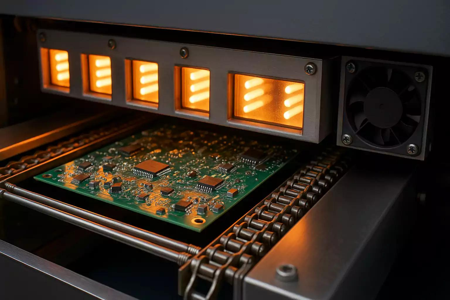
We handle fine-pitch and high-density assemblies, QFN and bottom-terminated parts, and BGA and micro-BGA down to 0.15 mm pitch. Each line carries 3D paste inspection, profiled reflow and 3D AOI, with X-ray close by.
Through-hole, mixed technology and special processes run in the same plant, so complex boards never leave the building. Supply parts yourself, or let us buy everything turnkey.
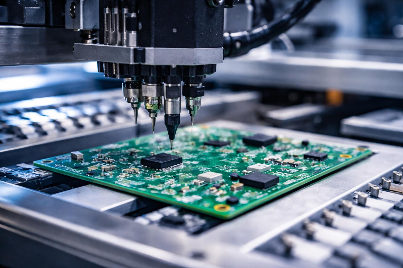
High-speed placement on Fuji AIMEX IIS and IIIC systems. The smallest component is 01005. Boards from 48 x 48 mm to 510 x 510 mm are handled, up to 6 mm thick.
Feeder capacity is 444 feeders plus 10 tray positions.
Conventional through-hole, large components, connector assemblies and mixed SMT plus PTH boards.
Selective wave, conventional wave and manual soldering cover the rest.
Rework, replacement and re-balling of BGA devices for repair and prototype work, under controlled process parameters and followed by re-inspection.
Automated MYCRONIC conformal coating applies protection selectively with thickness control. Thermal and environmental stress tests, including temperature cycling, verify reliability.
Taken from our capability sheet.
Incoming parts and reels are checked and kitted under control.
Paste is printed and measured in 3D.
Two placement stages, then nitrogen capable reflow.
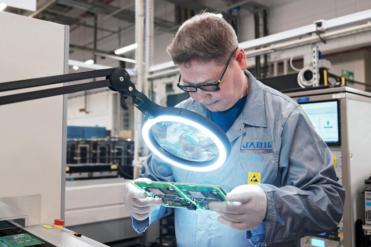
3D AOI, with X-ray wherever joints are hidden.
Through-hole, coating and functional or environmental testing.
01005 (0402 metric). Chip accuracy is ±50 µm and IC accuracy is ±30 µm
From 0.15 mm ball pitch up to 100 × 100 mm packages.
Full turnkey, partial turnkey and customer supplied material are all available.
With the Shimadzu X-ray system, which also supports first article inspection in house.