PCB Design
We lay out your schematic with layer stack-up, placement strategy, routing and controlled impedance planned together, up to HDI structures with blind, buried and stacked vias.
Rigid, flex and rigid-flex constructions are all in scope.
A board that looks right on screen can still be hard to build. Our engineers design and review with the production line in mind, so what you release is what the factory can make well.
Most manufacturing problems begin in the design file. A footprint slightly off, a stack-up nobody can build, a connector that will not solder cleanly. On screen they cost an afternoon. After material is ordered they cost weeks.
Our CAD and CAM engineers work from both sides of the problem. They know the behaviour of our SMT lines and fabrication partners, so spacing, panelisation, test access and part choices are right while the layout is still open.
Bring us an idea and we will design it, or bring a finished layout and we will review it. Either way you receive data the line can run without questions.
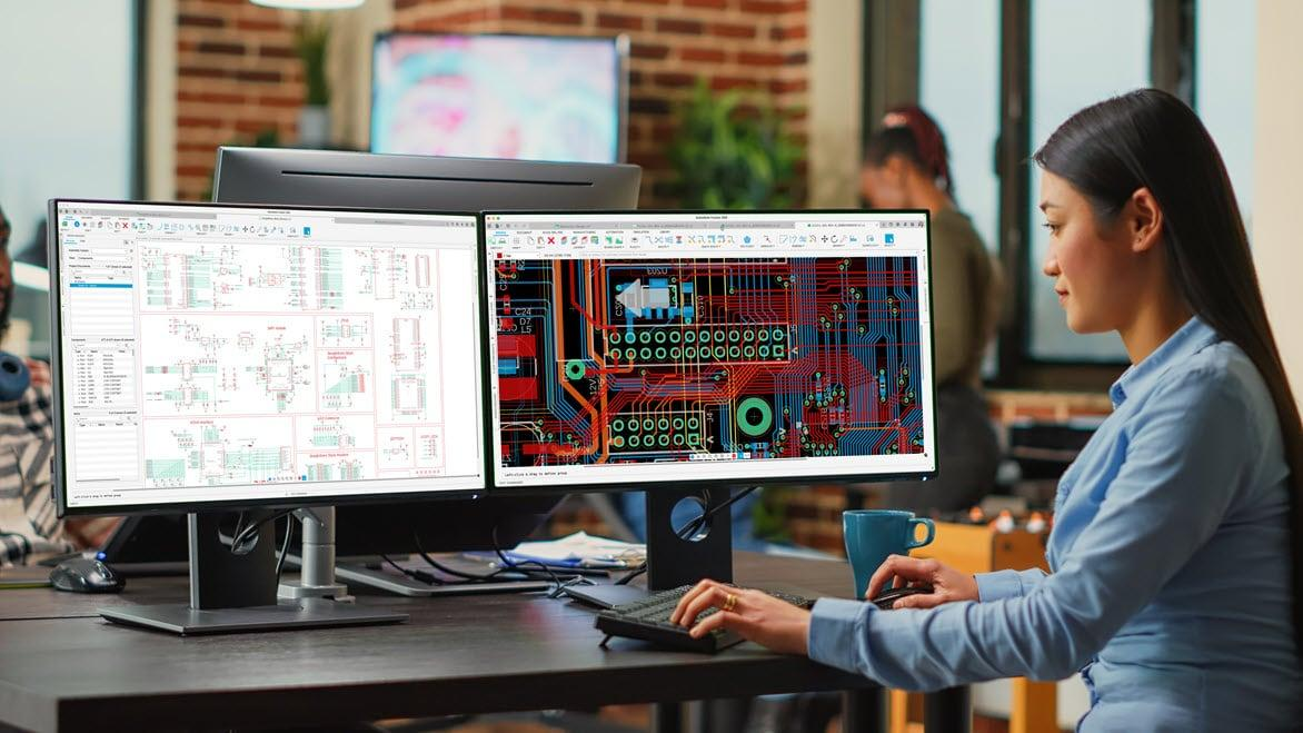
We lay out your schematic with layer stack-up, placement strategy, routing and controlled impedance planned together, up to HDI structures with blind, buried and stacked vias.
Rigid, flex and rigid-flex constructions are all in scope.
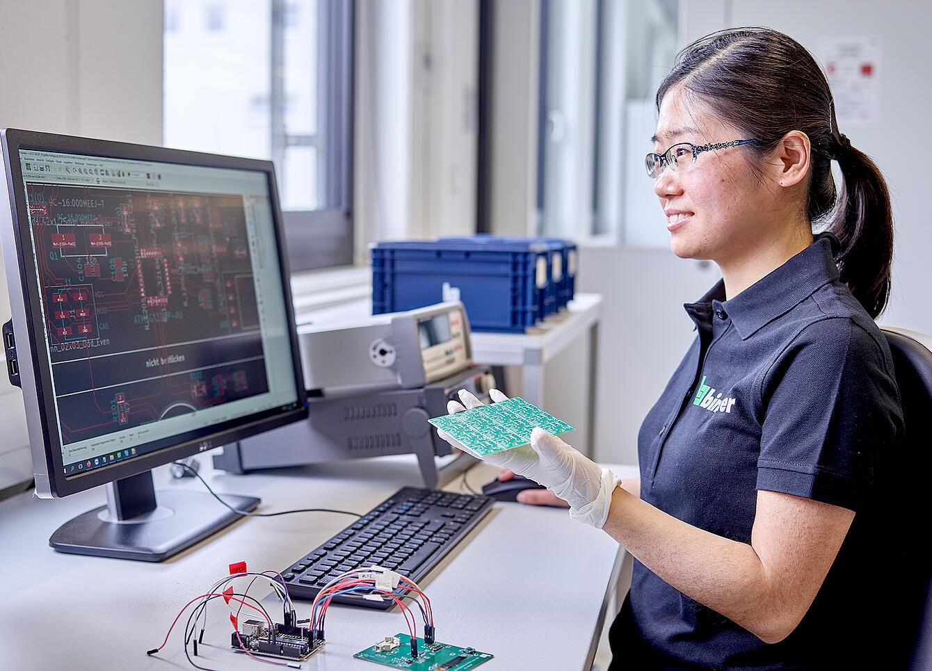
Before any release reaches the fabricator or the line, CAM engineers check the data: completeness, drill and via structure, solder mask, surface finish and panel layout.
You see the findings with the quote, before you commit.
We review how the board will actually be built and assembled: pad geometry, spacing, fiducials, paste apertures and reflow behaviour.
Each finding comes with a recommendation, so you change the design once and early.
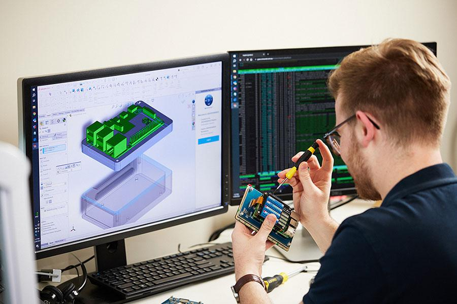
A board lives inside a product. We consider connectors, mounting, heat paths, enclosure and cable routing at the same time as the PCB.
That prevents the late surprise of a finished board that does not fit its housing.
Taken from our capability sheet.
Send your concept, schematic or finished files.
We create or review schematic, stack-up and layout.
You receive DFM, DFA and DFT findings with fixes.
We prepare data for fabrication and assembly.
Prototype and NPI help as the design reaches the line.
Yes. Send the files and our CAM team returns a manufacturability review with your quote.
Standard FR-4, high-speed and low-loss materials, and ultra-low-loss materials, with selection matched to the application.
Yes. Our engineering and NPI services cover prototype builds, process refinement and the move to volume.
Yes. Electromechanical design is part of the service, so the board is designed together with its surroundings.